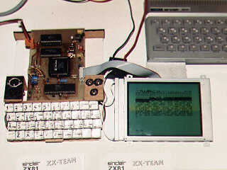
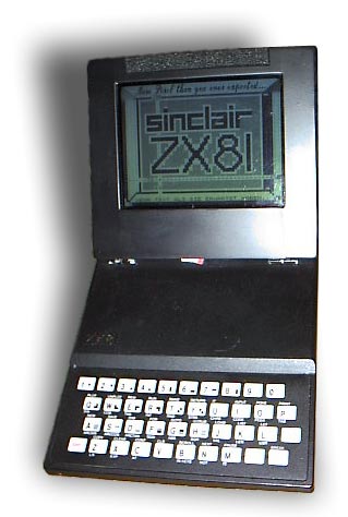
In 1997 I started learning VHDL at work. As an exercise I created this design with a Xilinx XC3042: an enhanced Sinclair ZX81, also known as Timex 1000. The added features are (in no special order) banked ROM, switchable RAM, separated busses, and a LCD interface. The current consumption is much less than the original so you can build a really neat laptop computer!
On this page you'll find only the sources and binaries for the FPGA and the CPU and few notes. To get a running system you need schematics, hardware, and some instructions. Please refer to the home page of the ZX-Team or the home page of Kai Fischer to get more information.
NOTE: The contents of this page will change some next time! Since there are at least two guys who are dealing with this design, I'm working now and then to give you more precise information here.
zx97src.zip Archive with source and binary configuration data for the FPGA design, 195KB.
zx97mngr.zip Archive with source and binary for the boot manager, 123KB.
The writing to 0000..1FFF will generate nor N_ROMCS neither N_RAMCS. Only read or refresh cycles enable the selects.
Coding of PAGE1/PAGE0 selects mapping of CPU 0000..1FFF: 00 = MEM 0000..1FFF, 01 = MEM 2000..3FFF, 10 = MEM 4000..5FFF, and 11 = MEM 6000..7FFF. ATTENTION: ROM 0000..0FFF are reserved for FPGA configuration, but can be tricked to be used for special programs as the boot manager.
Coding of RAM1/RAM0 selects mapping of RAM 2000..3FFF: 00 = nowhere, 01 = CPU 2000..3FFF, 10 = CPU A000..BFFF, and 11 = CPU A000..BFFF (additional RAM 4000..7FFF mirrored in CPU C000..FFFF.) CPU 4000..9FFF is always mapped to RAM.
Opcode fetches (M1 cycles) in CPU C000..FFFF start the video logic, the CPU gets 00 on data bus. The next refresh cycle generates the address for the pixel pattern. If in character mode (0000..1FFF resp. 3FFF) the address from the CPU is modified in the lower 9 bits. The byte read in will be shifted out as video signal.
To get some options switchable I use the address 0007H. If you write to this address (for example by POKE) the content of the ROM isn't changed but the configuration register of the FPGA.
| Bit | Default | Name | Description |
|---|---|---|---|
| 7 | 0 | RESET | reset CPU |
| 6 | 1 | ROM0 | use ROM for first 8K |
| 5 | KBD_COL3 | PAGE1 | msb page for first 8K |
| 4 | KBD_COL2 | PAGE0 | lsb page for first 8K |
| 3 | KBD_COL4 | V_INV | normal/inverse video |
| 2 | 0 | CHR13 | character generation upto 3FFF |
| 1 | KBD_COL1 | RAM1 | msb RAM mode |
| 0 | KBD_COL0 | RAM0 | lsb RAM mode |
If RESET is set to 1 the CPU will receive a reset signal. This is recommended when switching ROM banks. The bit is reset automatically.
The Bit ROM0 selects between ROM (1) or RAM (0).
Setting V_INV to 0 will invert the video signal. Looks well on some CRTs.
Setting CHR13 to 1 will disable HRG generation for CPU 2000..3FFF (refresh cycles) and enable character mode.

Back to my home page.
Comments and such stuff go to: [email protected]